Understanding the Basics of PCB Design: A Step-by-Step Guide
Professor Volt
February 18, 2026

Dive into the essentials of PCB design and learn how to create your own electronic circuits.
Understanding the Basics of PCB Design: A Step-by-Step Guide
Introduction to PCB Design
Hey there! Welcome to the fascinating world of PCB Design, where science meets creativity. If you're curious about how your favorite gadgets work or aspire to build your own electronics, you're in the right place.
Let’s kick things off with the basics. A Printed Circuit Board (PCB) is essentially the backbone of modern electronic devices. From your smartphone to your laptop, PCBs are everywhere. They’re those green boards with tiny electronic components soldered onto them, playing a crucial role in supporting and electrically connecting these components. Without them, our devices would be a jumbled mess of wires and parts!
Why Are PCBs So Important?
Imagine trying to connect all the components in a smartphone with individual wires - yikes! PCBs make it possible to design compact and reliable electronic circuits. They allow for:
- Miniaturization: Compact designs that save space.
- Reproducibility: Consistent manufacturing of devices.
- Durability: Stable support for components.
A Peek at the PCB Design Process
Designing a PCB is like solving a puzzle. It involves several steps:
- Schematic Capture: Drawing the circuit diagrams that represent how components connect.
- Component Placement: Positioning each component on the board strategically.
- Routing: Designing the paths or traces that connect the components electrically.
- Design Rule Check (DRC): Ensuring the design follows manufacturing specifications.
- Fabrication: Sending the design to be manufactured into a physical board.
Each of these steps requires attention to detail and a dash of creativity.
Who Is This Guide For?
Whether you’re a curious beginner looking to make your first DIY project or an advanced hobbyist ready to refine your skills, this guide is crafted with you in mind. We'll walk through each step of the PCB design process, offering practical examples and tips to get you comfortable with the basics.
The goal is simple: to help you understand the foundation of PCB design so you can bring your electronic ideas to life.
I can't wait to dive deeper with you! So grab a cup of coffee, and let's embark on this exciting journey together.
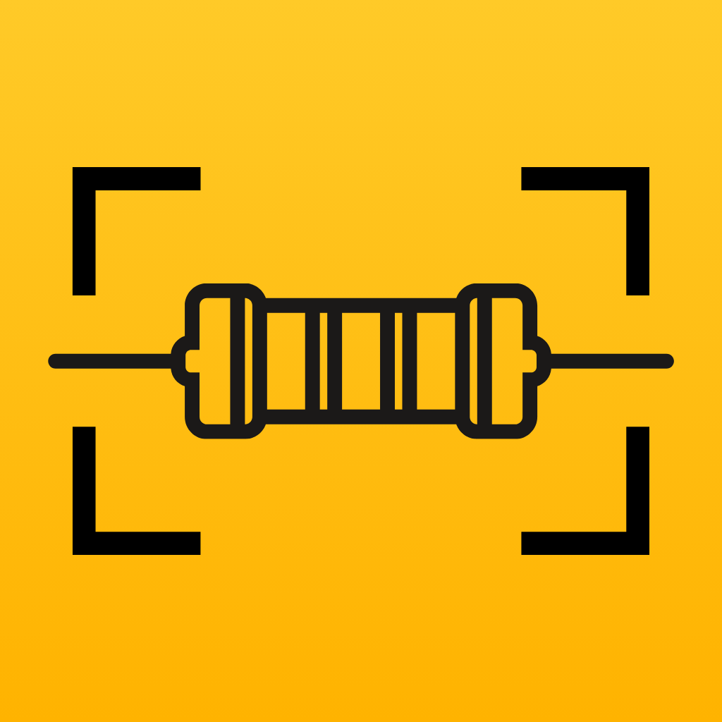
Try AI Resistor Scanner
Instantly identify resistor values with your camera
Essential Tools and Software for PCB Design
Alright, now that we've dipped our toes into the world of PCBs, let's dive into the tools of the trade! Whether you're just starting out or looking to upgrade your toolkit, having the right software and tools is crucial for effective PCB design. Trust me, having the right gear makes all the difference.
Popular PCB Design Software
When it comes to software, there's a buffet of options to choose from. Here are some of the most popular ones:
-
Eagle: A favorite among hobbyists and professionals alike, Eagle offers a robust set of features. It's particularly known for its schematic capture and PCB layout tools. Plus, it's part of the Autodesk family, which means excellent integration with other design tools.
-
KiCad: An open-source gem that's gaining popularity quickly. KiCad is free and offers a comprehensive suite for schematic capture and PCB layout. It's perfect for beginners who want to get their feet wet without splashing out on expensive software.
-
Altium Designer: The Rolls Royce of PCB design software. Altium Designer is packed with advanced features that make it ideal for complex, multi-layer boards. It's on the pricier side, but if you're serious about design, it’s worth the investment.
Basic Tools for PCB Design
Aside from software, let's not forget the basic tools that will accompany you on your PCB design journey:
-
Schematic Capture Tools: This is where it all begins. You'll use these tools to draw and simulate your circuit diagrams, ensuring everything works as expected before laying out the board.
-
Layout Tools: Once your schematic is ready, layout tools help you place components and route traces on the PCB. These tools are crucial for optimizing space and ensuring electrical integrity.
-
Design Rule Check (DRC) Tools: These are your best friends in catching errors before you send your design off for manufacturing. They'll help you adhere to manufacturing specs and avoid costly mistakes.
Free vs. Paid Software Options
You might be wondering, "Should I go for free software or invest in a paid option?" The choice largely depends on your needs and budget:
-
Free Software: Perfect for beginners. Options like KiCad offer a full-fledged design experience without the cost. They're ideal if you're experimenting or working on simple projects.
-
Paid Software: These typically offer more advanced features and support. If you’re planning on designing complex boards or working in a professional setting, investing in software like Altium Designer can save you time and headaches down the line.
Remember, every designer’s needs are different. Take the time to explore these tools and decide which fits your style and project requirements the best.
Think of these tools as your trusty sidekicks on your PCB design adventure. Choose wisely, and you'll be crafting masterpieces in no time!
Understanding PCB Design Terminology
Alright, folks! Now that we have a broad understanding of what a PCB is and why it’s important, it’s time to dive into some essential terminology. Don’t worry if these terms sound a bit technical. We’ll break them down so you can feel like a PCB design pro in no time!
Traces, Pads, and Vias
Let’s start with some of the most common terms you’ll encounter:
-
Traces: Think of traces as the highways of a PCB. They are the thin copper lines that electrically connect different components on the board. Just like highways, they need to be carefully planned to ensure that everything flows smoothly without congestion!
-
Pads: Pads are the spots where the components are soldered onto the PCB. Imagine them as parking spots for the components. They can come in different shapes and sizes, depending on the type of component being mounted.
-
Vias: When your traces need to travel between layers of a PCB, vias come into play. They are small holes filled with metal that allow electrical connections to pass from one layer to another. Think of them as underground tunnels connecting different layers of your highway system.
Layers of a PCB
Speaking of layers, let's talk about the difference between single-layer, double-layer, and multi-layer PCBs:
-
Single-layer PCB: As the name suggests, these PCBs have only one layer of conductive material. They are straightforward and typically used in simpler electronics like calculators or power supplies. They’re like a single-story house—easy to navigate but limited in space.
-
Double-layer PCB: With two layers of conductive material, these PCBs offer more flexibility. You can route traces on both sides, which is handy for more complex circuits. Imagine a two-story house with an additional floor to spread out your rooms.
-
Multi-layer PCB: These are the skyscrapers of the PCB world, featuring three or more layers. They are used in complex devices like computers and smartphones where space is a premium. Multi-layer PCBs allow for intricate designs and high-density connections, much like an office building packed with many floors of activity.
The Role of Gerber Files
Now, once your design is complete, you’ll need to communicate it to a manufacturer. Enter Gerber files. These are essentially the blueprints of your PCB design. They contain all the information required to fabricate the board, including the layout of traces, pads, and vias across various layers.
Gerber files are to PCBs what architectural plans are to buildings. They ensure that your PCB is manufactured exactly as you’ve envisioned it. Here’s a pro tip: always double-check your Gerber files for accuracy before sending them off to manufacture. A small mistake here could lead to costly errors!
Understanding these basics will set a solid foundation as you continue on your journey into the world of PCB design. Keep these terms in your back pocket, and you’ll navigate the PCB landscape with confidence!
Step-by-Step PCB Design Process
Welcome to the hands-on part of your PCB design journey! Whether you're building your first project or refining your skills, understanding the step-by-step process is key to success. This section will guide you through creating a schematic, designing a PCB layout, routing traces, and finalizing your design. Let’s dive in!
Creating a Schematic
The first step in designing a PCB is to create a schematic. Think of it as a blueprint for your circuit. It visually represents how each component connects with one another. Here’s how to get started:
-
Choose Your Design Software: There are various tools available like KiCad, Eagle, or Altium Designer. These tools help you draw and simulate your schematics.
-
Place Components: Use the software to place each component symbol on the schematic. Imagine you’re piecing together a jigsaw puzzle!
-
Connect the Dots: Draw wires to connect the components just like in your circuit diagram. This step ensures your components communicate correctly.
-
Annotate & Review: Add labels and values to each component. Double-check everything, just like proofreading an essay. Trust me, this saves headaches later!
Designing the PCB Layout
Now that you have a schematic, it’s time to convert it into a PCB layout. This involves defining the physical dimensions and positioning of components on the board.
-
Import the Schematic: Most software will allow you to import your schematic directly into the PCB layout editor.
-
Define the Board Outline: Set the board’s shape and size. A small project might look like a tiny rectangle, while a more complex one could have intricate shapes.
-
Place Components: Carefully position each component on the board. Keep related components close to reduce trace length and improve performance.
Routing the Traces
Routing is where the magic happens. It’s like drawing the roads that connect different cities (or components) on your board.
-
Plan Your Routes: Start by planning where your main traces will go. Consider power and ground paths first.
-
Use Auto-Router (or Manual): Some tools offer auto-routing features. However, manual routing gives you more control and often better results. It's akin to choosing between a guided tour and an adventure of your own making.
-
Keep Clearances in Mind: Ensure there is enough space between traces to prevent shorts. This is crucial for the board's reliability.
-
Optimize and Review: Go over your routes and optimize them for efficiency. Cut unnecessary angles and make your paths as direct as possible.
Finalizing the Design
You’re almost at the finish line! Finalizing your design involves a few critical checks.
-
Run Design Rule Checks (DRC): Your software can check for errors such as unconnected nets or clearance violations. This is like a spell-check for your PCB design.
-
Generate Gerber Files: These are the files you’ll send to a manufacturer. They contain all the information needed to fabricate your board.
-
Review & Revise: Before sending off your files, review everything. It’s better to catch mistakes now than after manufacturing!
By following these steps, you're well on your way to creating a functional and reliable PCB. Remember, practice makes perfect, and each project will enhance your skills. Happy designing!
Common Mistakes in PCB Design and How to Avoid Them
Hey there, PCB enthusiasts! It's time to chat about those pesky pitfalls in PCB design. Buckle up, because understanding these common mistakes can save you a lot of time, money, and frustration.
Incorrect Trace Widths
One of the most frequent blunders in PCB design is using incorrect trace widths. But why does this matter? Well, traces are like the veins of your PCB, carrying current between components. If they're too narrow, they can overheat and fail.
Best Practices
-
Calculate Current Requirements: Determine the amount of current each trace will carry and adjust its width accordingly. A handy tool for this is a trace width calculator. It's like a GPS for your PCB journey!
-
Refer to IPC Standards: The IPC-2221 is a go-to standard that provides guidelines on trace widths for different current levels.
Poor Component Placement
Ah, the art of component placement! It’s much more than just fitting pieces onto a board. Poor placement can lead to signal interference and inefficient routing.
Avoidance Strategies
-
Prioritize Functionality: Group components that interact closely with each other. Think of it like arranging a kitchen – you want the stove near the fridge, right?
-
Minimize Path Lengths: Keep the paths between related components as short as possible to reduce inductance and resistance.
-
Consider Thermal Management: Place heat-sensitive components away from heat-generating parts.
The Power of Design Rule Checks (DRC)
Think of Design Rule Checks (DRC) as your PCB's spellcheck. It’s a feature in most PCB design software that ensures your layout adheres to specific guidelines and constraints.
Why DRC is Crucial
-
Catch Errors Early: DRC can spot issues like trace spacing violations or incorrect hole sizes before you send your design off for fabrication.
-
Save Time and Money: By catching mistakes early, you avoid costly revisions and delays.
Final Thoughts
Mistakes in PCB design can be like gremlins, sneaking in when you least expect them. However, by being aware of these common pitfalls and using best practices, you can keep your designs sleek, efficient, and ready for the real world. So, next time you're in the design phase, remember these tips and use your DRC tool religiously. Your future self will thank you!
And hey, if you're just starting out or looking for tools to help with these aspects, check out some PCB design software options here. They're packed with features that make avoiding these mistakes easier. Happy designing!
Testing and Prototyping Your PCB Design
Alright, you've made it this far! By now, you've put a lot of thought into your PCB design, and it's looking pretty snazzy, right? But hold on a second before hitting the big red "produce" button. Prototyping is your best friend here, and trust me, it can save you a heap of headaches and dollars down the line.
Why Prototype First?
Think of prototyping as a dress rehearsal for your PCBs. It helps you:
- Identify Flaws: Catch any design issues or errors before mass production.
- Save Costs: Spotting mistakes early means less wasted material and time.
- Improve Design: You might notice areas to enhance or simplify.
I've been there myself. I once thought I had the perfect design for an LED matrix, only to find out during prototyping that I'd overlooked a crucial connection. A close call indeed!
Methods for Testing PCB Designs
When it comes to testing, you’ve got several tools in your toolbox:
Breadboards
These are fantastic for beginners and quick tests. A breadboard lets you build circuits without soldering, using jumper wires to make connections. It's a hands-on way to see your circuit live and catch any basic issues.
Simulation Software
If you're more of a digital native, simulation software is your go-to. Tools like LTspice or Altium Designer allow you to simulate how your circuit will behave. You can tweak and test without even touching a component. Plus, it's super satisfying to watch your digital circuit light up without a single piece of hardware in sight.
Rapid Prototyping Services
Once you’ve ironed out any kinks with breadboards or simulations, consider using a rapid prototyping service. These companies can quickly produce a small batch of your PCBs. Here’s why they rock:
- Speed: Get a physical prototype in days rather than weeks.
- Precision: Advanced machinery ensures high-quality boards.
- Iteration: Quickly test different versions of your design.
Services like PCBWay or JLCPCB offer affordable options for hobbyists and professionals alike. They’re like having a magic wand that turns your digital design into reality.
Before you know it, you'll be holding a sleek, functioning PCB in your hands, ready for the next stages of testing or small-scale deployment. And that's where the real magic happens!
Conclusion and Next Steps
Congratulations! You've made it to the end of our journey into the world of PCB Design. Let's take a moment to recap the key points we've covered throughout this guide.
We started by understanding the importance of PCBs and how they serve as the backbone for modern electronics, offering miniaturization, reproducibility, and durability. We then delved into the PCB design process, exploring each critical step—Schematic Capture, Component Placement, Routing, Design Rule Check (DRC), and finally, Fabrication. Each step is like a piece of a puzzle, fitting together to create the functional and reliable boards that power our favorite gadgets.
Now that you have a solid foundation, it's time to roll up your sleeves and put theory into practice. Start your own PCB design project! Whether you're crafting a simple LED circuit or embarking on a more complex design, the journey is both challenging and rewarding. Remember, every expert was once a beginner. Don't be afraid to make mistakes; they're part of the learning process.
To help you take your skills to the next level, here are some fantastic resources to explore further:
-
Online Courses: Platforms like Coursera and Udemy offer comprehensive courses on advanced PCB design techniques. These courses can provide in-depth knowledge and hands-on practice.
-
PCB Design Software Tutorials: Many PCB design tools, like KiCad and Eagle, come with built-in tutorials and user communities. Participating in forums can be a great way to learn from experienced designers and troubleshoot issues.
-
Books and E-books: Titles such as "The Circuit Designer’s Companion" by Peter Wilson can be invaluable for diving deep into the intricacies of PCB design.
-
YouTube Channels: Channels like "EEVblog" offer practical insights and project ideas that can inspire and guide you through the design process.
Don't forget to check out our recommended tools and resources here (affiliate link), where you can find everything you need to kickstart your PCB projects with ease.
In the end, PCB design is an art as much as it is a science. Let your creativity flow, and have fun experimenting with your designs. The world of electronics is vast and ever-evolving, and you've just taken your first steps into an exciting, limitless universe. Happy designing!